Solution
ASE FCBGA/WLCSP/LGA/DRQFN Package Service
Flip Chip BGA (FCBGA)
Flip Chip BGA (FCBGA)
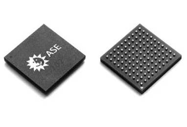
- Flip chip technology involves flipping the chip over and directly mounting it onto the substrate, as opposed to the conventional face-up mounting with wire bonds.
- The advantages of flip chip include the ability to shrink the chip size, resulting in higher signal density, and optimizing the circuit path to enhance electrical performance.
- PGC has a long-term cooperation with ASE, enabling us to offer the best-suited solutions to meet specific application requirements.

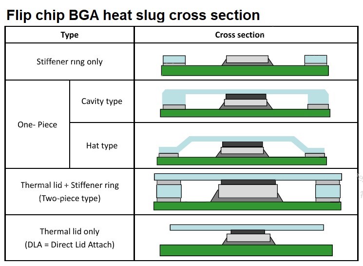
- Flip Chip BGA with heat slug thermally enhanced by adhering it to the rear side of the chip and the substrate. This method can effectively remove the heat and improve the thermal performance.
- There are several heat slug types, including hat type, cavity type, .. etc., as the illustration.
Flip Chip CSP (FCCSP)
Flip Chip CSP (FCCSP)
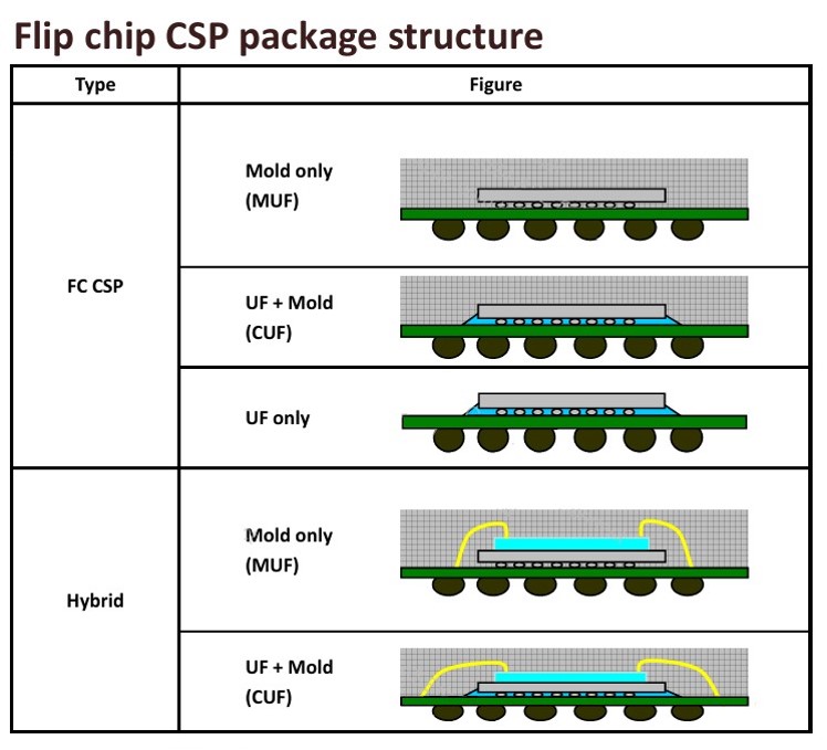
- FCCSP (Flip Chip Chip Scale Package) provides enhanced chip protection through molding and features a thin, small profile, and lightweight packaging.
- Comparable with Known Good Die (KGD) solutions, FCCSP excels in cost-efficient test and burn-in while delivering equivalent electrical performance by substitute underfill.
Wafer Level CSP (WLCSP)
Wafer Level CSP (WLCSP)
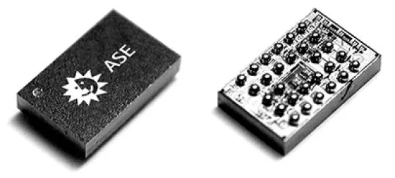
- WLCSP (Wafer Level Chip Scale Package) is an IC packaging technology performed at the wafer level. Unlike traditional procedures, WLCSP involves a bare die with a redistribution layer (RDL), interposer, or I/O pitch, which rearranges the pins or contacts on the die. This arrangement ensures that they are sufficiently large and spaced apart, thereby facilitating handling.
- The primary benefits of WLCSP include reduced package size, enhanced thermal conduction characteristics, and the absence of bond wires or interposer connections. It has been widely used in Bluetooth/Wi-Fi, cell phones, analog devices, power and voltage regulators, RF devices, .. etc.
Land Grid Array (LGA)
Land Grid Array (LGA)
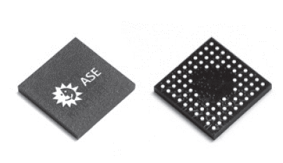
- LGA resembles BGA but lacks the solder balls, and offers distinct advantages over other leadless packages due to its flexible routing capabilities and support for multi-chip modules.
- Features
- .Thinner(down to 0.5 mm), lighter and smaller CSP
- .Mature standard matrix BGA assembly process with higher quality, lower cost
- .Space reduction in system level
Dual Row QFN (DRQFN)
Dual Row QFN (DRQFN)
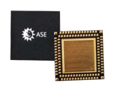
- The Dual-Row is designed to increase the lead counts to meet specific product requirements.
- Both rows of leads can be connected to the die using wire bonds.
- Features
- .Small footprint(No require formed perimeter leads)
- .Light weight
- .Excellent thermal/electrical performance
- .Better power dissipation
