Solution

Gate Array Turnkey Service

0.35um GATE ARRAY BODIES @TSMC/VIS FAB

0.35um GATE ARRAY BODIES
@TSMC /VIS FAB

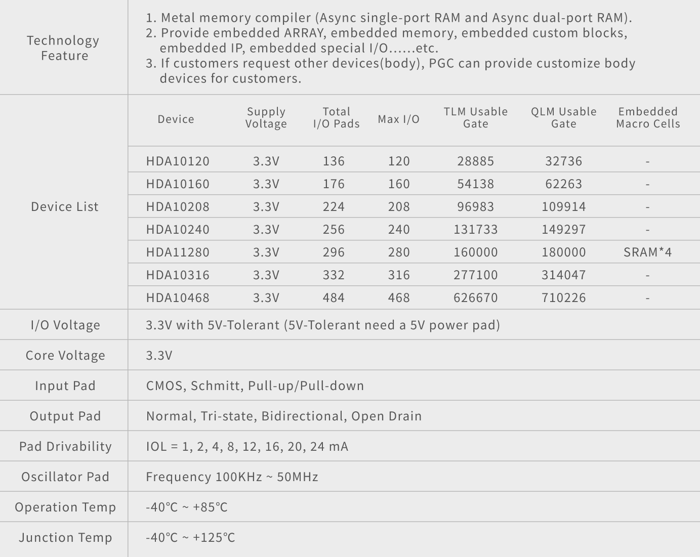
HDA10000 Products 0.35um
5V Tolerant I/O, 3.3V Process, Stagger I/O
8″ wafer TSMC FAB

“Support Special MoQ”

Note:
1. Usable gates are estimated; the actual number of usable gates is design dependent.
2. I/O pads can be used as VDD/VSS pads.
3. There are four (4) dedicated VDD/VSS pads for each corner cell in the chip.

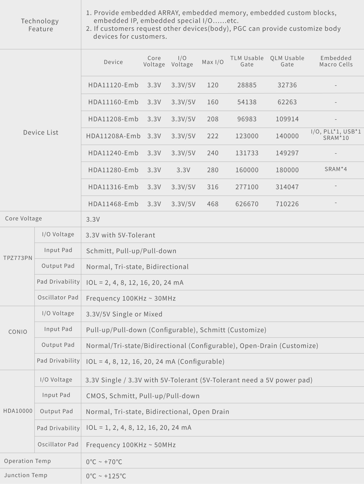
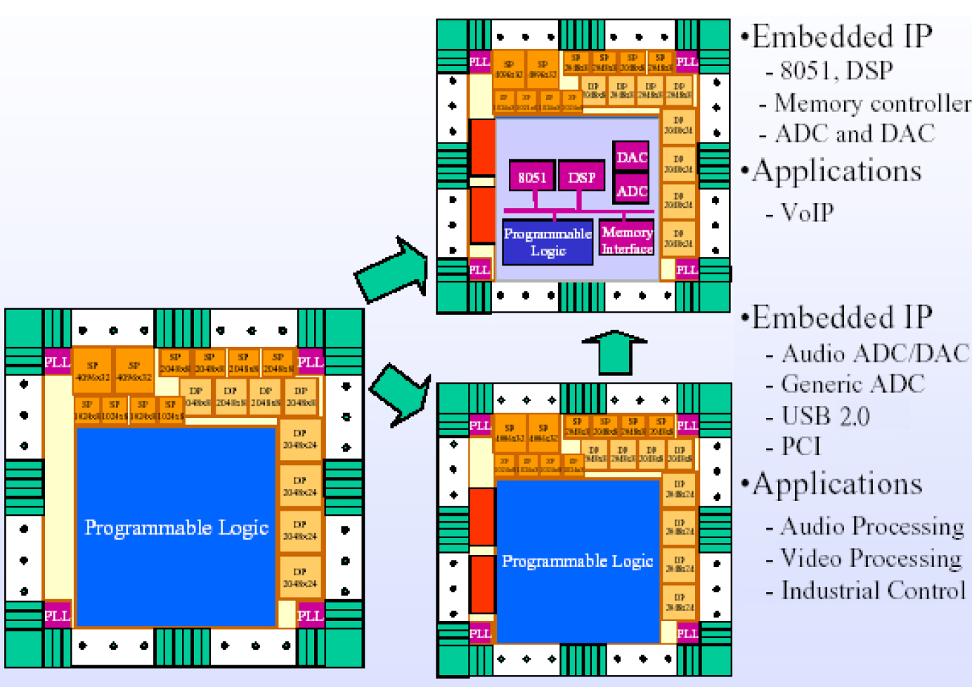
ASPEC 0.35um Embedded Array: HDA11000-Emb Product

ASPEC 0.35um Embedded Array:
HDA11000-Emb Product

8″ wafer TSMC FAB

“Support Special MoQ”

Note:
1. Usable gates are estimated; the actual number of usable gates is design dependent.
2. I/O pads can be used as VDD/VSS pads.
3. Used ASPEC logic IP for Embedded array.

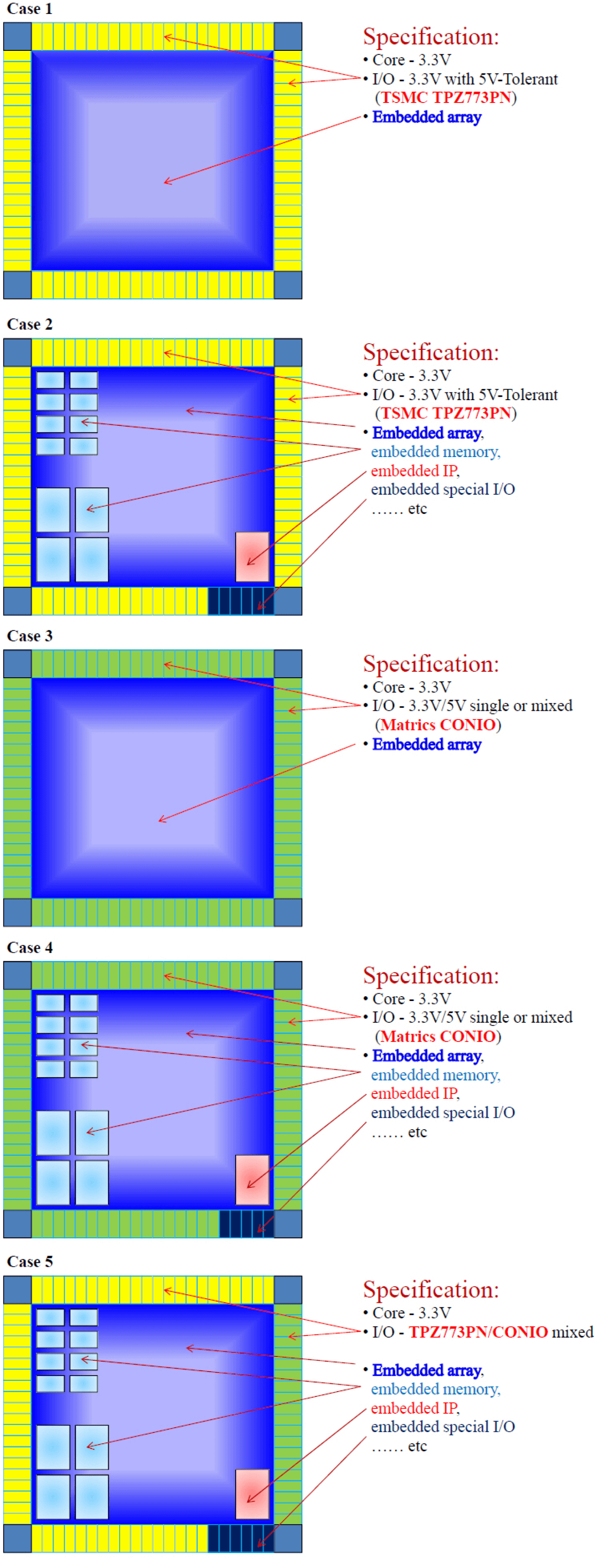
ASPEC 0.35um Embedded Array: Application

ASPEC 0.35um Embedded Array:
Application

0.5um GATE ARRAY BODIES @TSMC/VIS FAB

0.5um GATE ARRAY BODIES @TSMC/VIS FAB

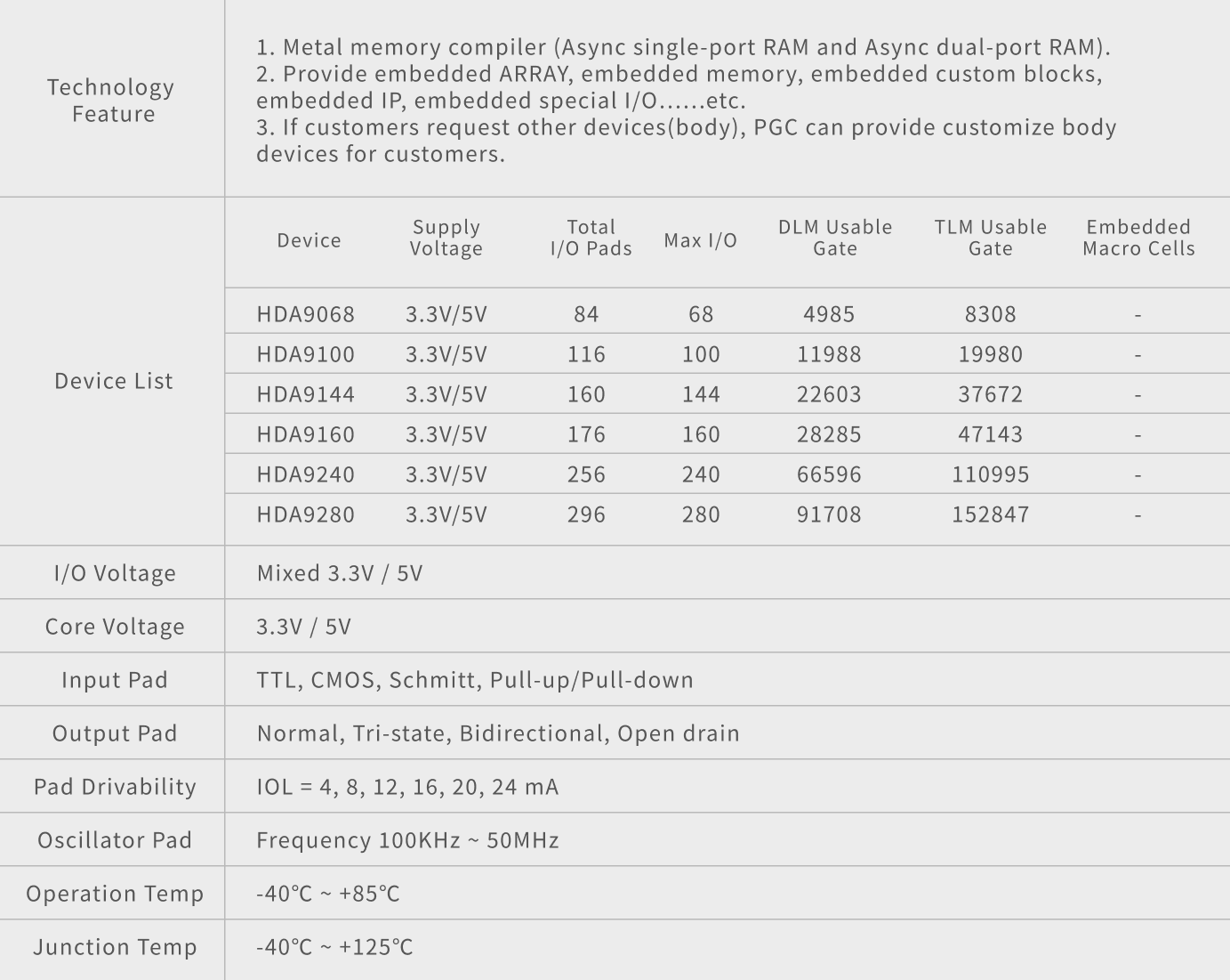
HDA9000 Products 0.5um
Mixed 3V/5V Power, 5V Process Core: 3V/5V, Stagger I/O
6″/8″ wafer TSMC/VIS FAB

“Support Special MoQ”

Note:
1. Usable gates are estimated; the actual number of usable gates is design dependent.
2. I/O pads can be used as VDD/VSS pads.
3. There are four (4) dedicated VDD/VSS pads for each corner cell in the chip.

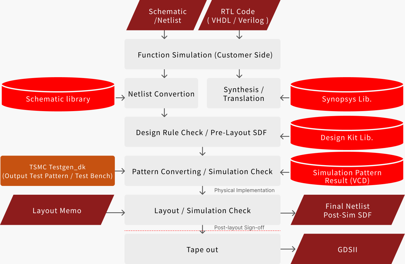
Gate Array Design Flow

Gate Array Design Flow

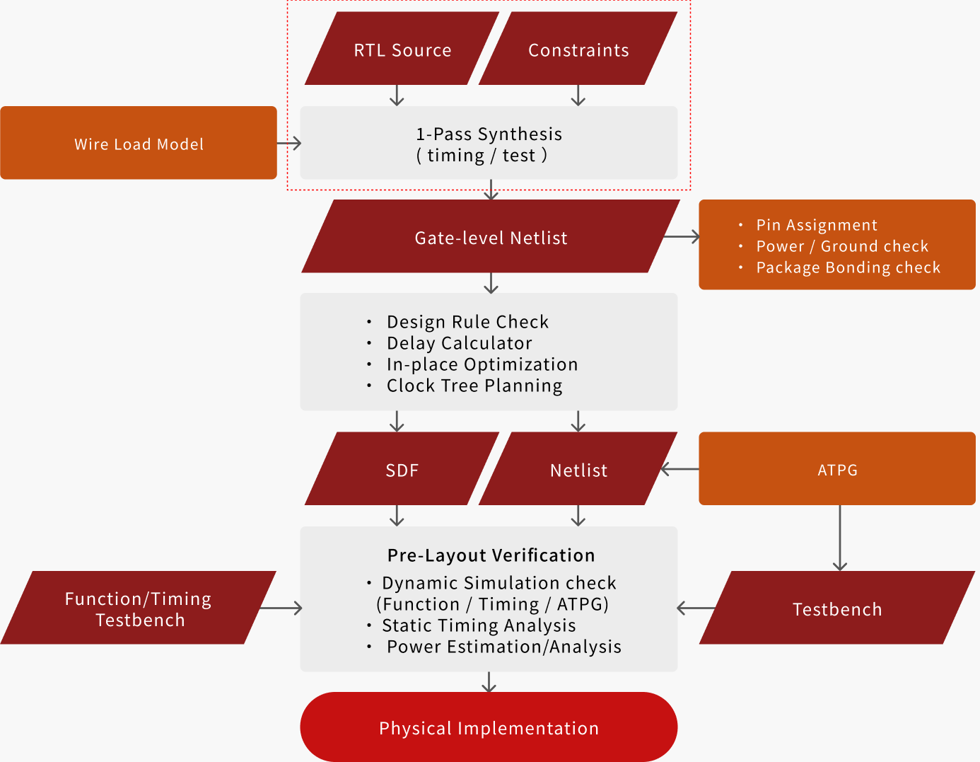
RTL to Netlist Flow

RTL to Netlist Flow

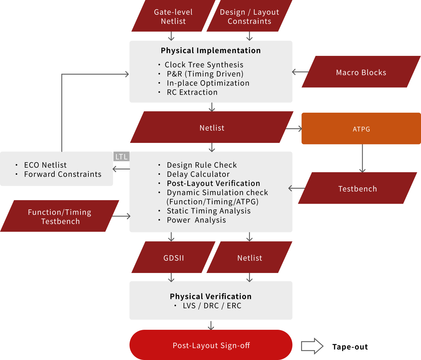
Netlist to Tape Out Flow

Netlist to Tape Out Flow

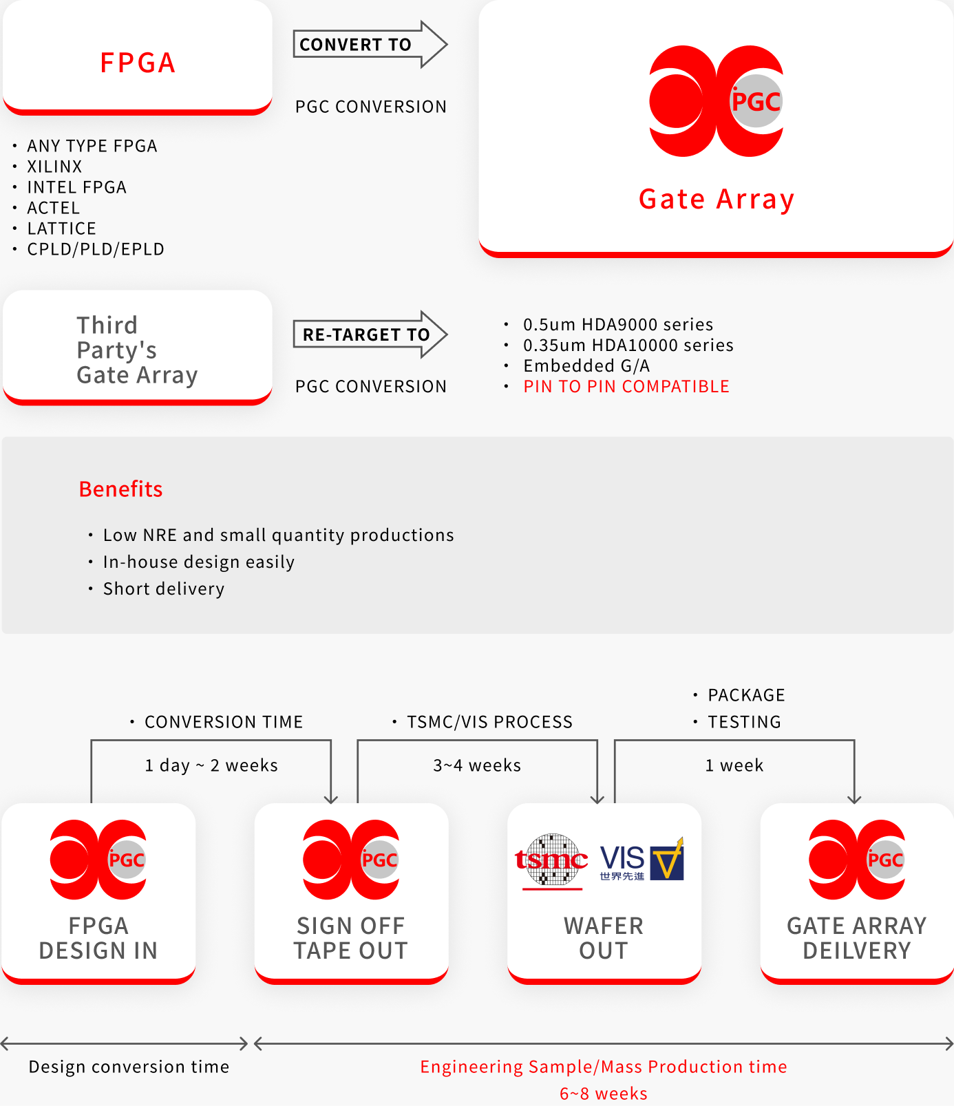
FPGA → Gate Array Conversion

FPGA → Gate Array Conversion

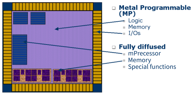
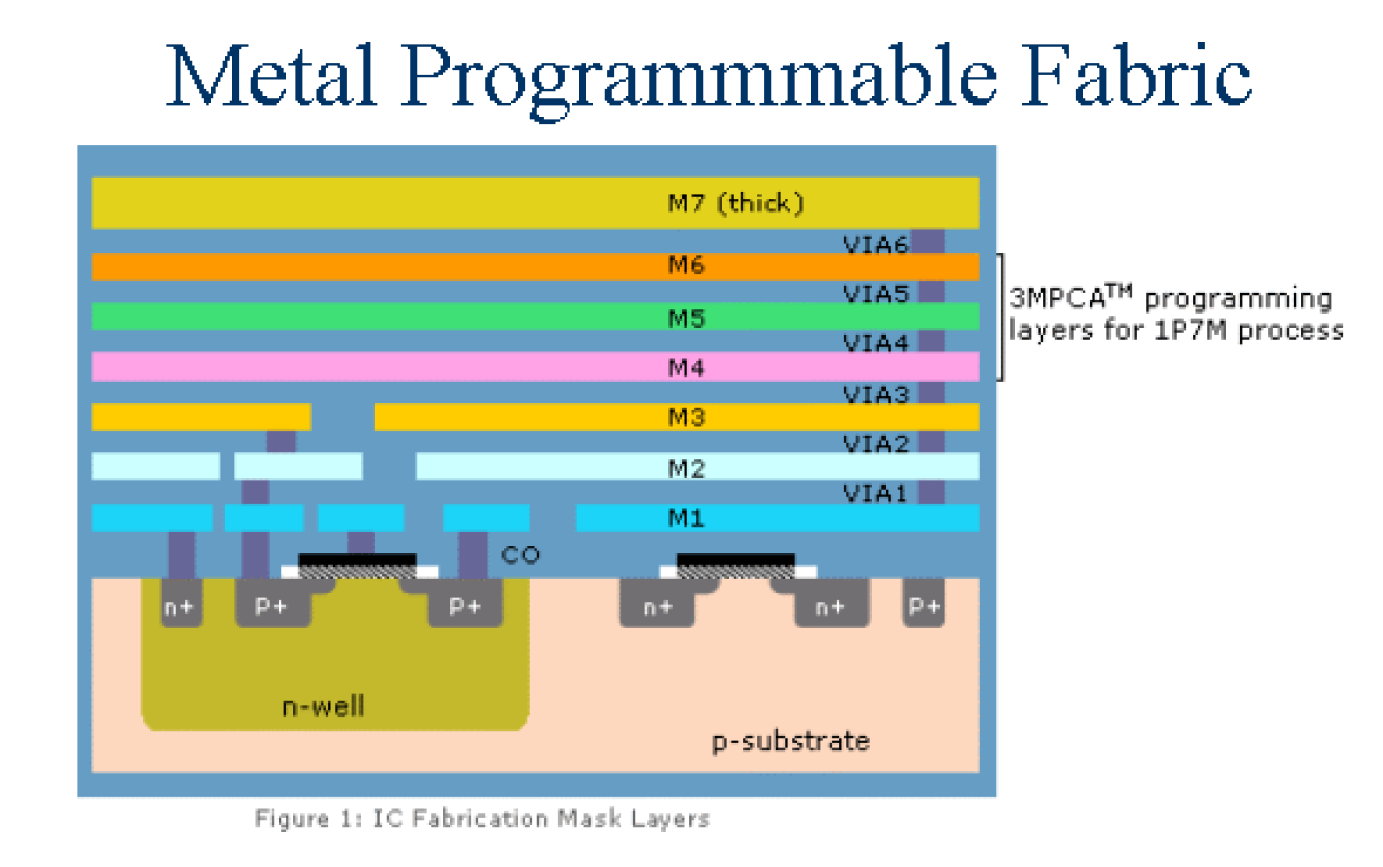
Structured ASIC IP (0.13um, 0.18um)

Structured ASIC IP
(0.13um, 0.18um)

Scroll to Top