Note: 1. Usable gates are estimated; the actual number of usable gates is design dependent. 2. I/O pads can be used as VDD/VSS pads. 3. There are four (4) dedicated VDD/VSS pads for each corner cell in the chip.
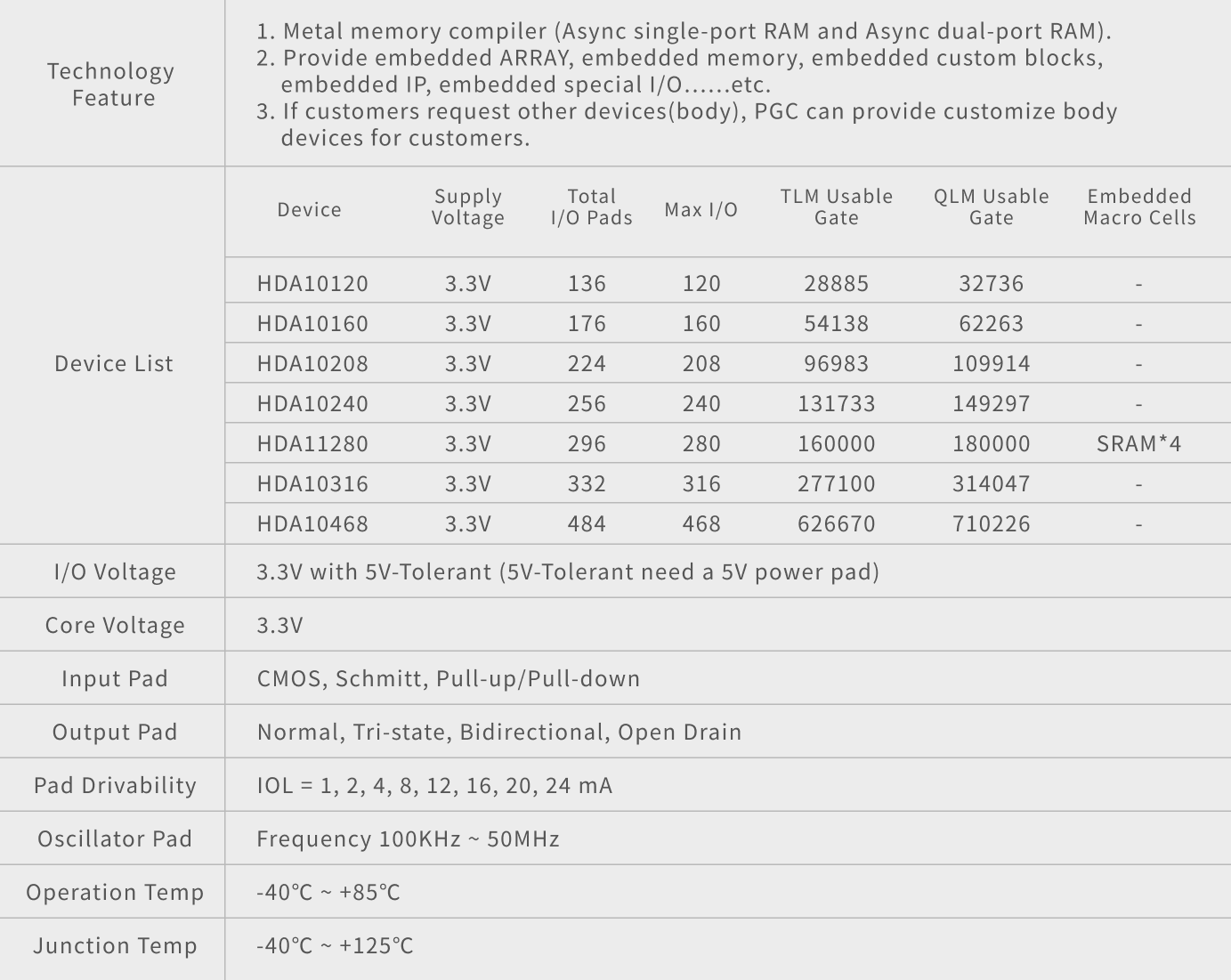
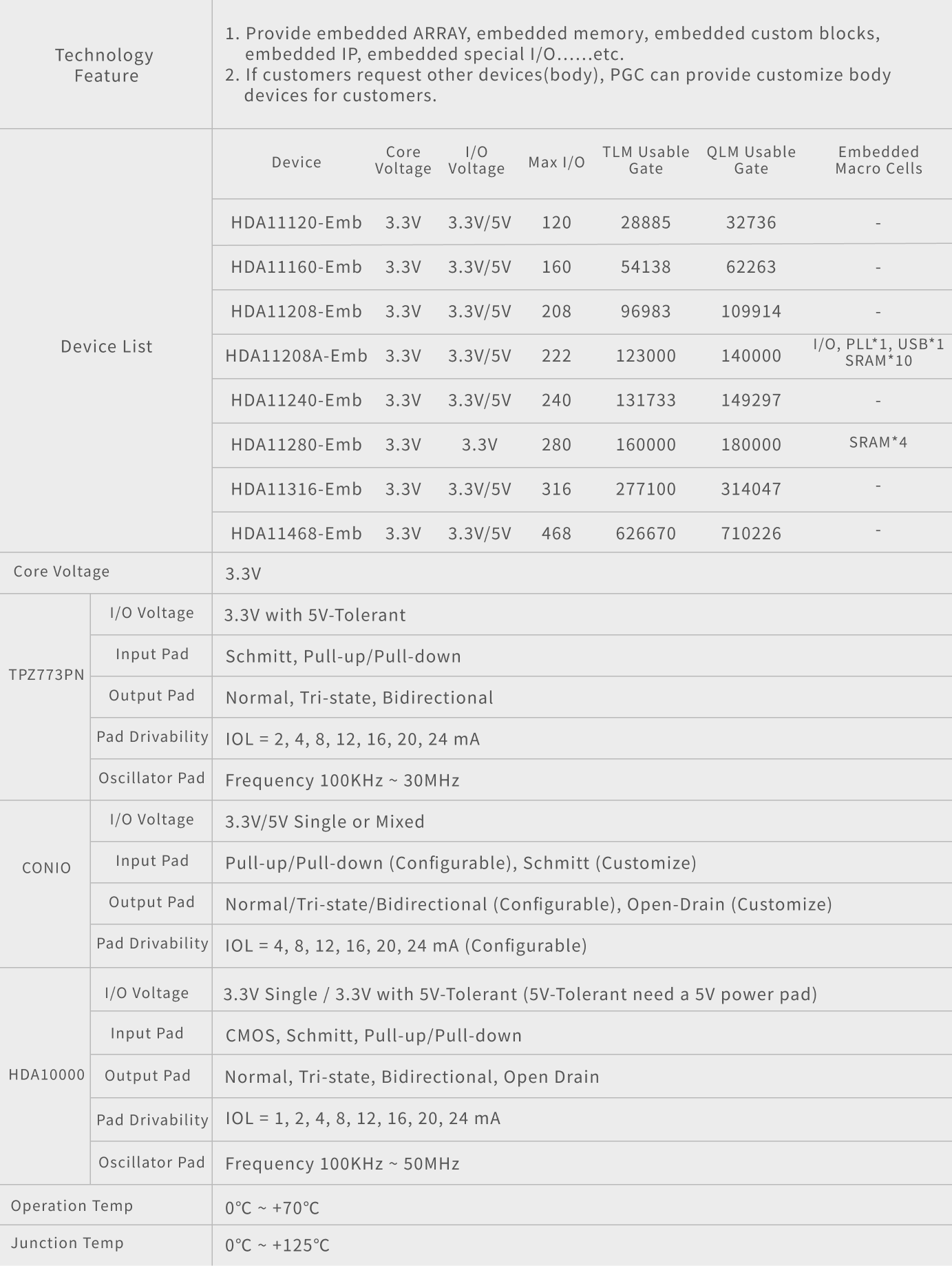
Note: 1. Usable gates are estimated; the actual number of usable gates is design dependent. 2. I/O pads can be used as VDD/VSS pads. 3. Used ASPEC logic IP for Embedded array.
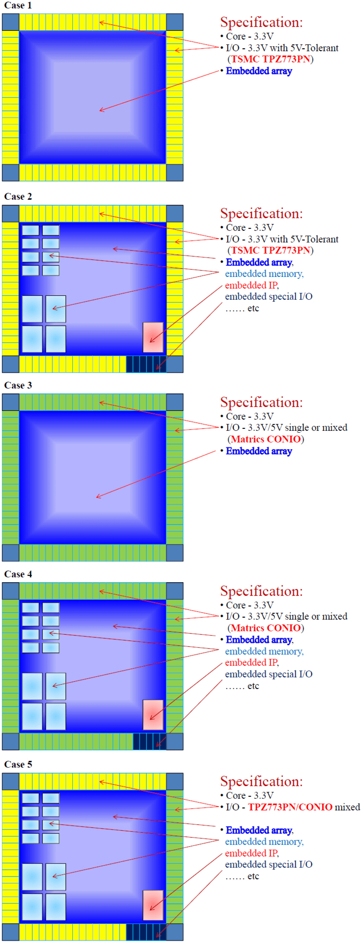
ASPEC 0.35um Embedded Array: Application
ASPEC 0.35um Embedded Array: Application
0.5um GATE ARRAY BODIES @TSMC/VIS FAB
0.5um GATE ARRAY BODIES @TSMC/VIS FAB
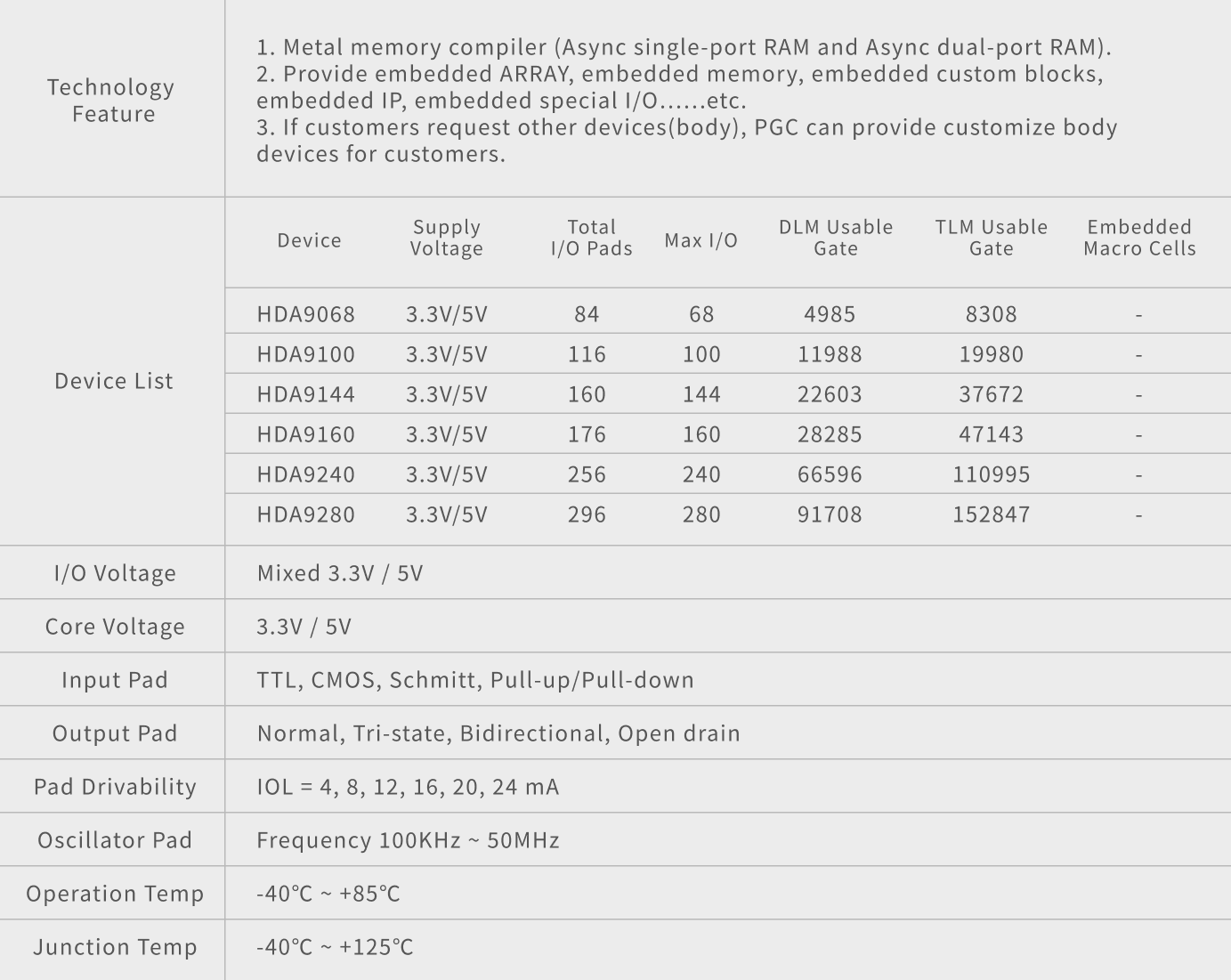
HDA9000 Products 0.5um Mixed 3V/5V Power, 5V Process Core: 3V/5V, Stagger I/O 6″/8″ wafer TSMC/VIS FAB
Note: 1. Usable gates are estimated; the actual number of usable gates is design dependent. 2. I/O pads can be used as VDD/VSS pads. 3. There are four (4) dedicated VDD/VSS pads for each corner cell in the chip.
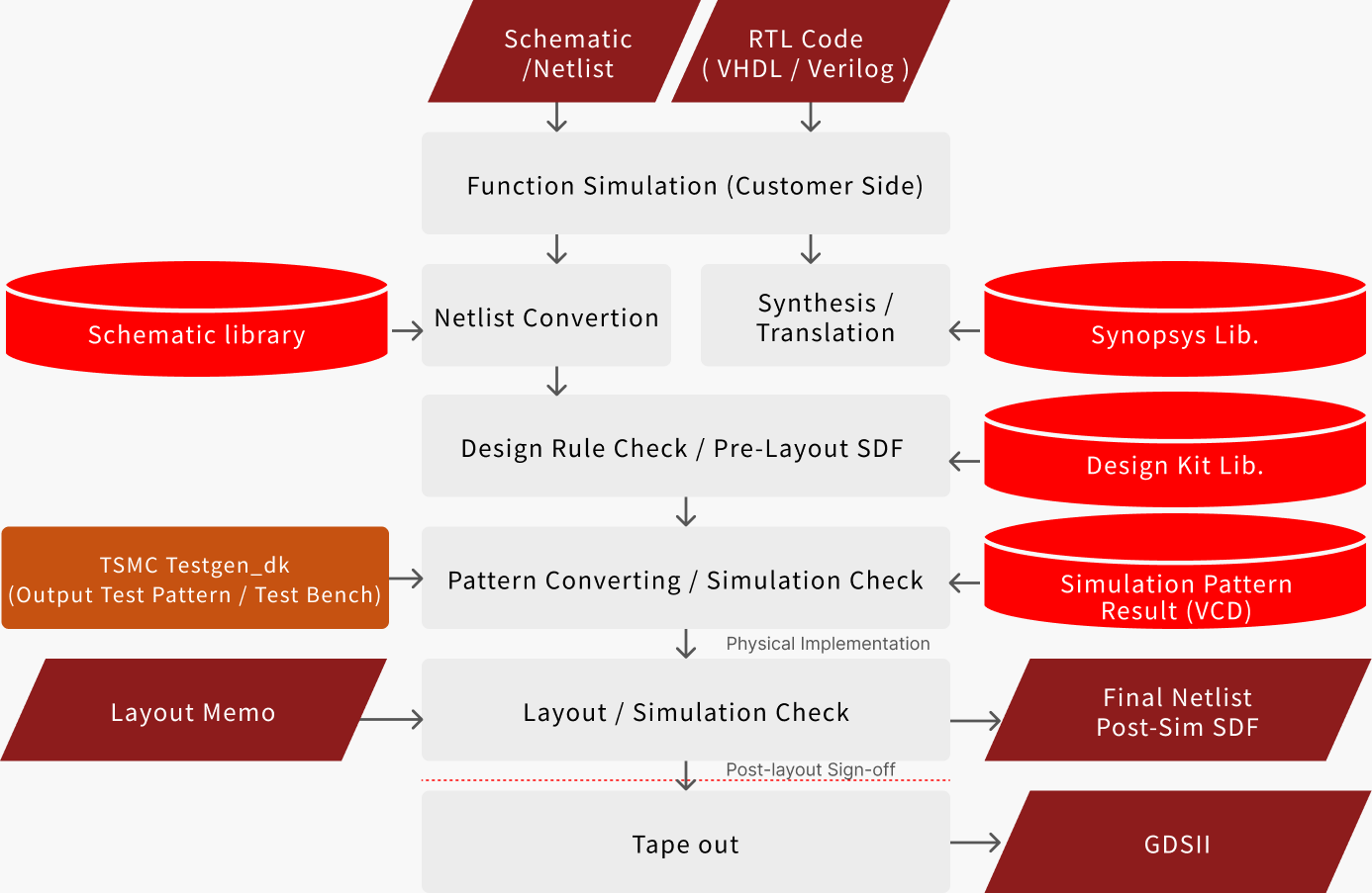
Gate Array Design Flow
Gate Array Design Flow
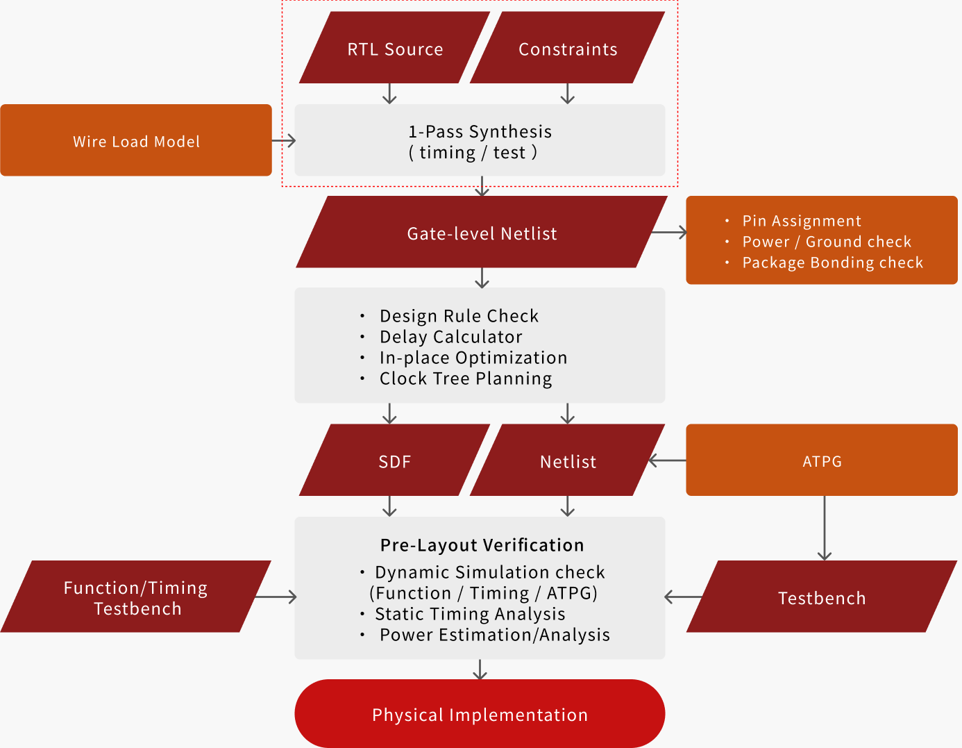
RTL to Netlist Flow
RTL to Netlist Flow
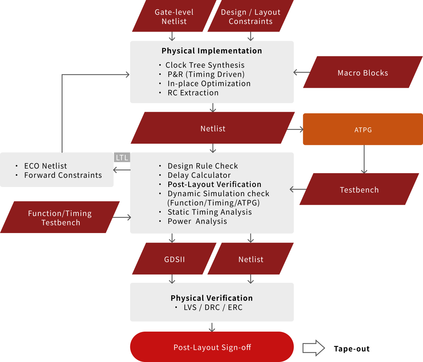
Netlist to Tape Out Flow
Netlist to Tape Out Flow
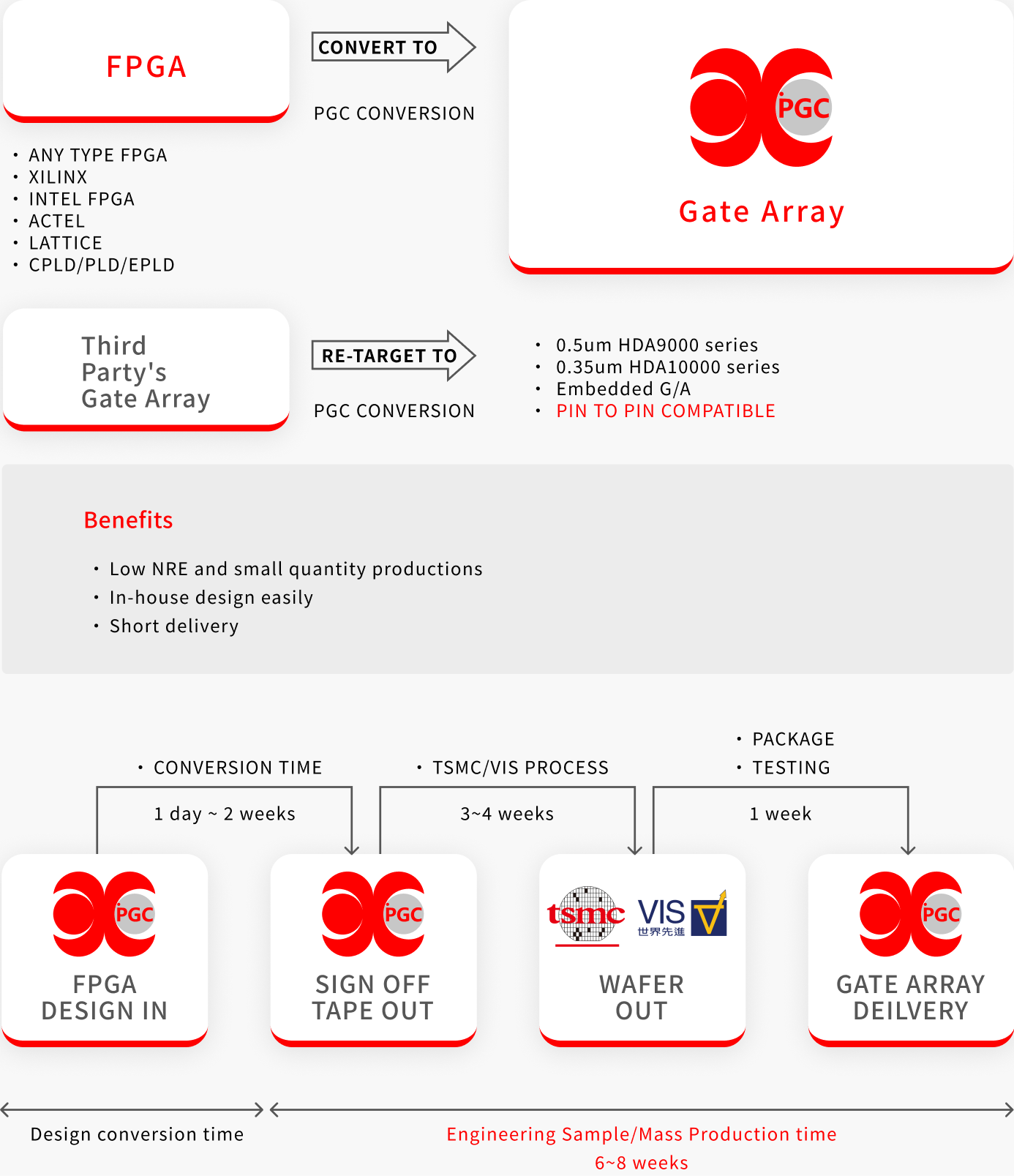
FPGA → Gate Array Conversion
FPGA → Gate Array Conversion
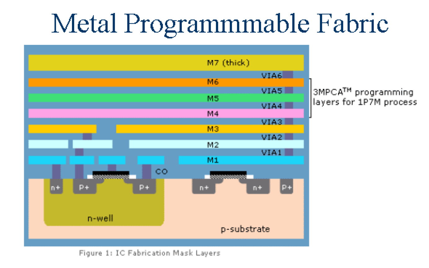
Structured ASIC IP (0.13um, 0.18um)
Structured ASIC IP (0.13um, 0.18um)
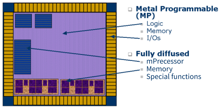
FPGA like architecture
Split-the-Middle choice (ASIC/FPGA)
Predefined logic array/config. memory
Pad limited design
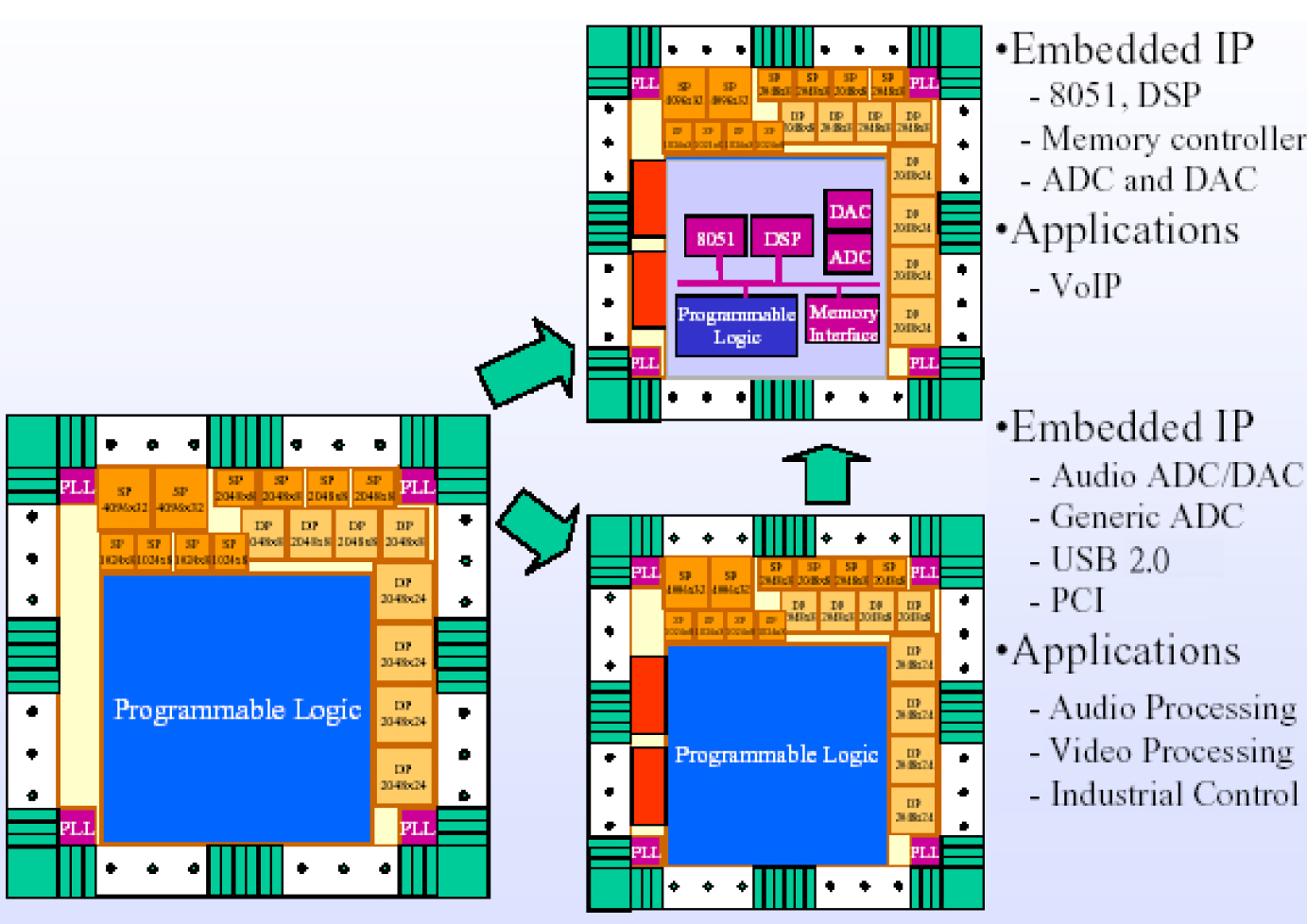
Embedded Silicon IP
Platform ASIC (CPU, high speed) Integration
Clock domain
Preconfigured DFT (scan, BIST)
Power distribution
返回頂端
本網站使用cookies以提昇您的使用體驗及統計網路流量相關資料,繼續使用本網站表示您同意我們使用cookies。我們的隱私權政策提供更多關於 cookies 使用及停用的相關資訊。我同意隱私權政策